
利用SATA接口中P11信号扩展硬盘指示灯
如需对单个硬盘进行状态监测,或扩展一些超本没有硬盘读写信号指示灯时可行的解决办法。
要获取SATALED single首先想到的是sata的控制芯片(也就是芯片组),针对intel 7系主板,可查阅相关文档(7-series-chipset-pch-datasheet.pdf)。由于芯片组采用BGA封装,并且信号引脚在主板上难以查找,所以无法接线获得。
进而考虑到硬盘驱动器估计有相关的读写壮态信号,以方便监测。所以查询SATA接口定义文档(HIGH SPEED SERIALIZED AT ATTACHMENT(sata).pdf)。
l P11--Device Activity Signal
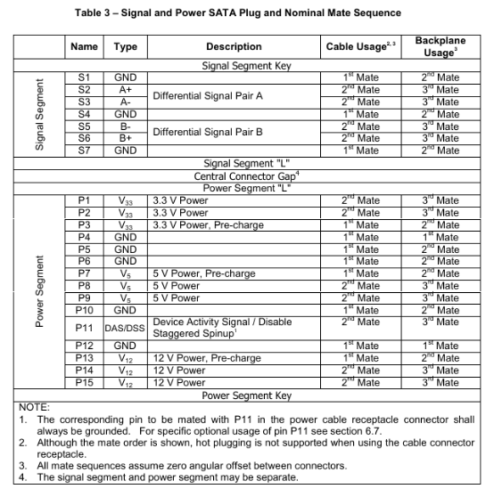
注意:在实际情下,PC电源提供的电源接头直接将p10,p11,p12短路接地,使得p11处于 “Disable Staggered Spinup”状态(无用,都使用芯片组提供的信号),有一些连黄线(3.3v)也不接。但笔记本是呼一20mA般不短接。所以先确定给SATA硬盘供电的接口没有将p11接地,不然就要自行处理了。

Pin11 — Device Activity Signal
Electrical Definition:
The signal the device provides for activity indication is a low-voltage low-current driver intended
for efficient integration into current and future IC manufacturing processes. The signal is not suitable for directly driving an LED and shall first be buffered using a circuit external to the device before driving an LED.
The activity signal is based on an open-collector or open-drain active-low driver. The device shall
tolerate the activity signal being shorted to ground. The device shall tolerate a no-connect floating
activity signal.
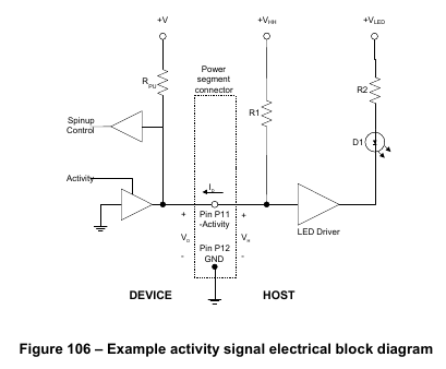
如上所述,活动信号是基于一个集电极开路或漏极开路低电平驱动。P11的电压和电流不能直接驱动,需要扩展电路来驱动LED。
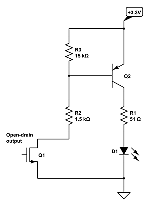
电路比划(设计谈不上)
由于是业余,对以上指标一知半解。加上的电子元件的来源是费电子产品(鼠标、网卡),所以电扩展电路的设计更是有什么用什么,元件的标量更是有什么用什么,与赤脚医生抓药一样,不烧硬盘就试试看,边做边调节。最终得此电路方子。

该电路实现了当硬盘读写工作时,p11给出漏极开路低电平,相当于p11接地(所以在测试电路时,不用真接硬盘,通过模拟接地就好了)。此时,T1的Ic电流增大,让LED熄灭。即:LED常亮,读写时灭。与常见表示方法反过来。
该电路的设计原则:
l R1 > Vcc(3.3/5v) / 0.3uA
l R2 ≈ (Vcc – 2.4) / 0.02a
n usually in the range 1.8V to 2.4V for red LEDs, and 3V to 4.2V for blue, white, and high efficiency green LEDs, 20mA
n 140Ω for the 5V supply case, and 55Ω for the 3.3v
l R3 目标是使p11 的电压控制在1.8v – 2.1v 之间。
l T1 只要是个低压三极管就用,在数字电路中,大多三极管都应该是开关三极管吧。K72没找到,在破网卡上找到这样S2A.
最后连接的面包析也没用,只好临时借用破鼠标的电路板正面开始对贴片元件进行拼接。

、
最终在实际笔记硬盘上投入使用。能用就很満足了,合理化还要专业人士来做。
参考资料:
http://electronics.stackexchange.com/questions/44923/driving-a-led-with-an-open-drain-digital-input
edit
If the output can’t sink enough current you’ll need an external transistor to increase that.
If the output is active (low) there will flow a 1.5 mA from +3.3 V through Q2’s emitter-base junction, R2 and Q1. That 1.5 mA will allow Q2 to source more than 100 mA for a typical general-purpose transistor. You will only get about 22 mA, though, because R1 won’t allow more.
If Q1 is off there won’t be any base current through Q1, so the LED will remain off. Q1 will have a small leakage current, and to avoid that this would get amplified by Q2 I added R3. As long as the leakage current is less than 0.7 V / 15 kΩ = 50 µA all the leakage current will flow through R3, so that will ensure Q2 will be completely off.